Author Affiliations
Abstract
State Key Laboratory on Integrated Optoelectronics, Institute of Semiconductors, Chinese Academy of Sciences, Beijing 100083, China
We report a compact 2×2 Mach–Zehnder interferometer (MZI) electro-optic switch fabricated on a silicon-on-insulator using standard complementary metal-oxide semiconductor (CMOS) processes. With a short modulation arm length of 200 μm, the crosstalk is reduced to 22 dB by the new modulation scheme of push–pull modulation with a pre-biased π/2 phase shift. The new modulation scheme can also work with a fast switching time of about 5.4 ns.
130.4815 Optical switching devices 130.3120 Integrated optics devices 200.4650 Optical interconnects Chinese Optics Letters
2015, 13(6): 061301

Author Affiliations
Abstract
1 Wuhan National Laboratory for Optoelectronics, Huazhong University of Science and Technology, Wuhan 430074, China
2 Institute of Semiconductors, Chinese Academy of Sciences, Beijing 100083, China
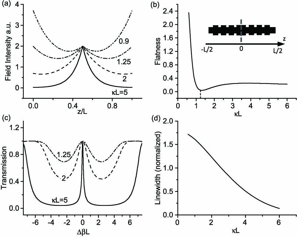
We demonstrate a large-mode-volume transverse-electric-polarized λ/4 shifted distributed feedback (DFB) cavity on silicon-on-insulator (SOI). A 2.86 mm-long DFB cavity with sidewall corrugation on the ridge is fabricated on a silicon rib waveguide. The cavity structure is designed to enlarge both the longitudinal and transversal mode profiles of the cavity to enclose more luminescent media. Design strategies are verified by both finite difference time domain simulation and experiments. A linewidth of 69 pm and an extinction ratio of 15 dB is obtained, indicating not only the well confinement of the longitudinal mode, but also its well stretching to the cavity ends. The mode volume is 75.39 μm3.
130.0130 Integrated optics 130.7408 Wavelength filtering devices Chinese Optics Letters
2015, 13(10): 101301
1 武汉邮电科学研究院, 武汉430074
2 中国移动通信集团湖北有限公司, 武汉430023
硅基光互连技术是解决目前电互连制约瓶颈的有效手段, 而实用化集成光源的制备对硅基芯片功耗的降低和尺寸的减小有着十分重要的意义。硅基集成激光器在过去的十多年间取得了一系列重要突破, 其中III-V/Si混合集成激光器是近期最可能获得实际应用的方案之一。文章简要分析了硅基集成激光器的研究现状, 重点介绍了III-V/Si混合集成激光器的研究进展, 包括III-V/Si键合激光器和III-V/Si倒装焊激光器的发展和各自存在的问题, 并预测了硅基集成激光器的发展方向。
光互连 硅基激光器 混合集成 optical interconnect silicon-based laser hybrid integration
State Key Laboratory on Integrated Optoelectronics, Institute of Semiconductors (IS), Chinese Academy of Sciences (CAS), Beijing 100083, China
Frontiers of Optoelectronics
2012, 5(1): 90
State Key Laboratory on Integrated Optoelectronics, Institute of Semiconductors, Chinese Academy of Sciences, Beijing 100083, China
Frontiers of Optoelectronics
2011, 4(3): 282
Author Affiliations
Abstract
State Key Laboratory on Integrated Optoelectronics, Institute of Semiconductors, Chinese Academy of Sciences, Beijing 100083, China
We demonstrate a sub-nanosecond electro-optical switch with low crosstalk in a silicon-on-insulator (SOI) dual-coupled micro-ring embedded with p-i-n diodes. A crosstalk of -23 dB is obtained in the 20 \mu m-radius micro-ring with the well-designing asymmetric dual-coupling structure. By optimizations of the doping profiles and the fabrication processes, the sub-nanosecond switch-on/off time of <400 ps is finally realized under an electrical pre-emphasized driving signal. This compact and fast-response micro-ring switch, which can be fabricated by complementary metal oxide semiconductor (CMOS) compatible technologies, have enormous potential in optical interconnects of multicore networks-on-chip.
绝缘体上的硅 微环 电光调制器 等离子色散效应 光互连 130.3120 Integrated optics devices 250.6715 Switching 230.5750 Resonators 230.4000 Microstructure fabrication Chinese Optics Letters
2010, 8(8): 757
Author Affiliations
Abstract
1 State Key Laboratory of Modern Optical Instrumentation, Zhejiang University, Hangzhou 310027, China
2 State Key Laboratory of Integrated Optoelectronics, Institute of Semiconductors, Chinese Academy of Science, Beijing 10083, China
Pure Ge is grown on Si substrate to control the release of the strain in the heterostructure, which is due to the 4.2% lattice misfit between Ge and Si. In this letter, an innovative approach of multi-buffer layers is proposed for the epitaxial growth of high quality Ge thin films on Si (001) substrates in a molecular beam epitaxy system. The multi-buffer layers, including the low temperature Ge seed layer and the Si-Ge alloy intermediate layer fabricated under different temperatures, serve as defect gathering and annihilating sites to reduce the dislocation density in the top layers. The result reveals that the total thickness of the whole structure is less than 400 nm, with a low threading dislocation density of less than 5×105 cm-2 in the top layer and a root mean square surface roughness of 1.5 nm.
高质量锗薄膜 硅锗插入层 低温锗缓冲层 310.1860 Deposition and fabrication 310.6845 Thin film devices and applications 310.6870 Thin films, other properties Chinese Optics Letters
2010, 8(s1): 91
Author Affiliations
Abstract
State Key Laboratory on Integrated Optoelectronics, Institute of Semiconductors, Chinese Academy of Sciences, Beijing 100083
A 3-dB paired interference (PI) optical coupler in silicon-on-insulator (SOI) based on rib waveguides with trapezoidal cross section was designed with simulation by a modified finite-difference beam propagation method (FD-BPM) and fabricated by potassium hydroxide (KOH) anisotropic chemical wet etching. Theoretically, tolerances of width, length, and port distance are more than 1, 100, and 1 microns, respectively. Smooth interface was obtained with the propagation loss of 1.1 dB/cm at the wavelength of 1.55 microns. The coupler has a good uniformity of 0.2 dB and low excess loss of less than 2 dB.
集成光学 绝缘体上的硅(SOI) 多模干涉 配对干涉 耦合器 250.5300 Photonic integrated circuits 130.2790 Guided waves 220.4610 Optical fabrication Chinese Optics Letters
2007, 5(4): 215
中国科学院半导体研究所,集成光电子国家重点联合实验室,北京 100083
利用高阶Pade近似的2D-BPM算法,对具有不同弯曲半径及交叉角度的SOI弯曲交叉波导的传输特性进行了模拟、分析和深入研究,发现交叉波导的串扰随弯曲半径及交叉角度增大而减小的规律.在此基础上,对由正弦弯曲、余弦弯曲以及圆弧弯曲三种弯曲波导构成的SOI交叉波导的损耗及串扰特性进行了分析比较.结果表明,由正弦弯曲构成的交叉波导传输损耗最小且串扰最小.
导波光学 交叉波导 弯曲波导 Guided wave optics Silicon-on-insulator (SOI) SOI Intersecting waveguide Waveguide bend
State Key Laboratory on Integrated optoelectronics,Institute of Semiconductors, Chinese Academy of Sciences, Beijing 100083, CHN


